
This website uses cookies so that we can provide you with the best user experience possible. Cookie information is stored in your browser and performs functions such as recognising you when you return to our website and helping our team to understand which sections of the website you find most interesting and useful.
Multi-layers
Fully automated production workflows, precision registration processes and reliable through-hole plating guarantee the optimum quality of our products.
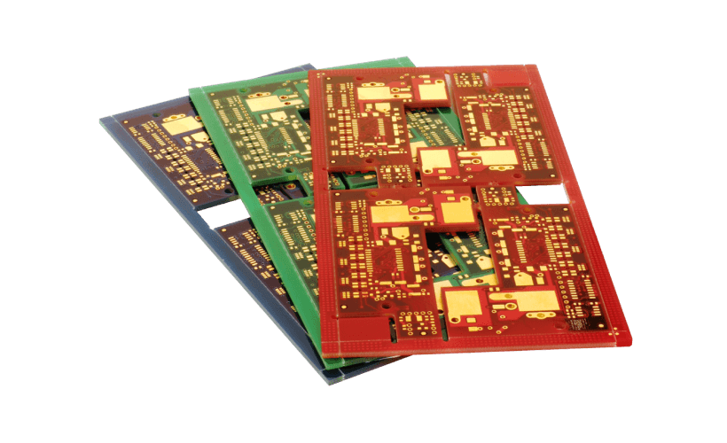
Multi-layer PCBs make it possible to separate analogue and digital sections on a single PCB. Today’s multi-layer circuits are characterised by ultra-thin cores, very small structures and an increased number of layers.
Features
Capabilities
Layers
max. 36 Layers
Laminate
FR4, High Tg FR4, Halogen free FR4, G10, BT, P97, PTFE
Thickness
0.2 to 7.0mm
Copper thickness
12/18/35/70/105µm
Approval
UL-approval, Flame class 94V-0, Class 1/2/3
Specialized laminate
Taconic, Rogers, Neltec, Arlon, further specialized materia
max. Boardsize
max. 610 x 730mm
Surface finish
Hot air leveling, (Lead or Lead-free)
Bondgold for ultrasonic bonding
Bondgold for thermalsonic bonding
Hardgold for Connectors
immersion Tin
chem. Au/Ni (immersion gold over nickel)
Silver ink or Carbon ink
OSP (Entek)
Soldermask
Liquid, photoimageable Mask, in green or any color Peelable
Mask
Component marking
White or per request
Outlines
CNC-Routing
CNC V-Scoring
CNC Milling
Laser Milling
min. Via Diameter
75µm (Laser), 100µm (Mechanical)
General tolerances
min. Outline tolerances routed
min. Holesize diameter
min. Hole position tolerance
min. Pattern Registration tolerance
min. Soldermask Registration tolerance
+/-0.075mm
+/-0.050mm
+/-0.050mm
+/-0.050mm
+/-0.050mm
General Capabilities
min. Annular ring
min. Soldermask bridge
plated Gold thickness
immersion gold thickness
Twist and Wrap
E/Test Voltage
Continuity
Flying Probe test available
Capped Vias
0.025mm
0.050mm
0.025µm – 3µm
0.025µm – 0.6µm
< 1%
24V – 300V
5 – 100Ohms