
This website uses cookies so that we can provide you with the best user experience possible. Cookie information is stored in your browser and performs functions such as recognising you when you return to our website and helping our team to understand which sections of the website you find most interesting and useful.
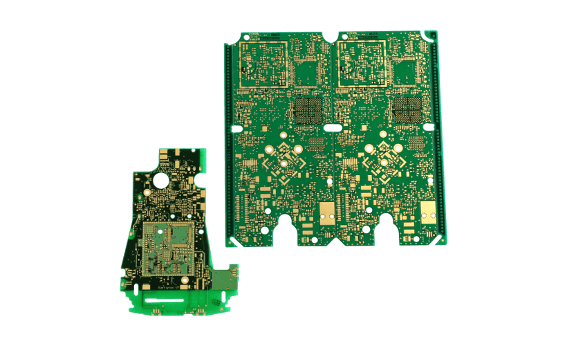
HDI PCBs
Thinner, smaller, lighter and more functions: This is the aim when developing and designing new components. The increased packing densities of components such as BGAs demand new layout structures. Based on laser via technology or controlled mechanical depth drilling, the connections to the inner layers can be produced based on staggered or stacked technology.
The latest production technologies in sterile areas and a team of top-qualified specialists in all production technologies are the basis for your customised HDI PCB.
The aim of every product development is a reliable solution which is tailored to the area of application, customised and perfect in terms of design and functionality.
Features
Capabilities
Layers
1+N+1 up to max. 4+N+4
Laminate
FR4, High Tg FR4, Halogen free FR4, G10, BT, P97, PTFE
Thickness
0.2 to 4.2mm
Copper thickness
12 / 18 / 35 / 70µm
Approval
UL-approval, Flame class 94V-0
Specialized laminate
Taconic, Rogers, Neltec, Arlon, further specialized material
max. Boardsize
max. 640 x 540mm
Surface finish
Hot air leveling, (Lead or Lead-free)
Bondgold for ultrasonic bonding
Bondgold for thermalsonic bonding
Hardgold for Connectors
immersion Tin
chem. Au /Ni (immersion gold over nickel)
Silver ink or Carbon ink
OSP (Entek)
Soldermask
Liquid, photoimageable Soldermask, in green or as requested
Peelable Mask
Component marking
White or per request
Outlines
CNC-Routing
CNC V-Scoring
CNC Milling
Laser Milling
min. Via Diameter
75µm (Laser), 100µm (Mechanical)
General tolerances
min. Outline tolerances routed
min. Holesize diameter
min. Hole position tolerance
min. Pattern Registration tolerance
min. Soldermask Registration tolerance
+/-0.075mm
+/-0.050mm
+/-0.050mm
+/-0.050mm
+/-0.050mm
General Capabilities
min. Annular ring
min. Soldermask bridge
plated Gold thickness
immersion gold thickness
Twist and Wrap
E/Test Voltage
Continuity
Flying Probe test available
Capped vias
0.025mm
0.050mm
0.025µm – 3µm
0.025µm – 0.6µm
< 1%
24V – 300V
5 – 100Ohms